NGK presents research findings on SiC wafers at ICSCRM2025
NGK Insulators (NGK) will participate in the International Conference on Silicon Carbide and Related Materials (ICSCRM) 2025, to be held in Busan, Republic of Korea, from Sunday, September 14 to Friday, September 19, 2025. We will present our research findings on Silicon Carbide (SiC) wafers used in next-generation power semiconductor devices. Additionally, we will exhibit related products.
Conference Overview
| Conference Name | International Conference on Silicon Carbide and Related Materials (ICSCRM) 2025 |
|---|---|
| City / Country | Busan, Republic of Korea |
| Venue | BEXCO - Convention Hall, Exhibition Center 1 Hall #1, Auditorium |
| NGK booth | Booth No.053 |
| Official Website | ICSCRM2025 CONFERENCEOpen new window |
| Dates | September 14 (Sun) to 19 (Fri), 2025 |
Presentation Overview
Oral Presentation
| Date and Time | September 19 (Fri), 2025, 14:00-14:15 |
|---|---|
| Room No. | Convention Hall A+B, 1F (FRI_3A) |
| Title | Reduction of Basal Plane Dislocations in 8-inch SiC Substrates Using Novel Crystal Growth Method Based on Batch Processing |
| Presenters | Hiroshi Fukui*, Yohei Okada, Yuki Urata, Shinya Matsukawa, Yutaka Nikai, Yusuke Tachida, Haruko Inayoshi, Kiyoshi Matsushima, Jun Yoshikawa |
| Presentation Summary | Reduction of basal plane dislocations (BPDs) in SiC substrates is an important issue to improve yield and reliability of SiC power devices. NGK has been developing a novel method to grow SiC single crystal layers with low BPD densities on multiple substrates by utilizing its ceramic processing technologies. As wafer diameters continue to increase in the SiC market, 8-inch wafers are expected to become the mainstream standard. In this presentation, we will introduce the basic characteristics of crystals produced using our fabrication method on 8-inch wafers, including BPD density. |
- *Oral Speaker
Poster Presentation
| Date and Time | September 18 (Thu), 2025, 15:00-17:00 |
|---|---|
| Location | Exhibition Hall 1, 1F at BEXCO (P20) |
| Title | Suppression of Bipolar Degradation in SiC PiN Diodes Using Substrates Fabricated by Novel Crystal Growth Method Based on Batch Processing |
| Presenters | NGK: Haruko Inayoshi*, Tomohiko Sugiyama, Kiyoshi Matsushima, Jun Yoshikawa NITech: Zhang Endong, Masashi Kato |
| Presentation Summary | To ensure the reliability of SiC power devices, suppression of bipolar degradation which originates from BPDs is one of the most important issues. To solve this issue, NGK has developed a novel crystal growth method to produce low BPD density substrate. In this presentation, we report the results demonstrating the suppression of bipolar degradation in PiN diodes using SiC substrates grown by this novel method. (This work is a result of joint research between Nagoya Institute of Technology and NGK Insulators.) |
- *Speaker
Exhibited Products
Silicon Carbide (SiC) wafer
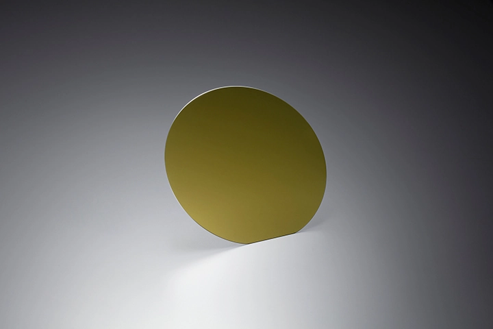
Silicon carbide (SiC) wafers are used in the manufacture of SiC power semiconductors used in electric vehicles (EVs) and other applications.
NGK applies a proprietary crystal growth method to achieve lower dislocation density in its SiC wafers, making it possible to provide high-quality SiC wafers that improve the reliability and lower the cost of the power devices used in inverters for EVs and other applications.
- About Silicon carbide (SiC) wafer
R&D Sample:
Large Current Ceramic Wiring Board
Large Current Ceramic Wiring Board is a new solution for wiring connections, which reduces switching surges and enables full-speed operation of SiC power devices by embedded thick Cu conductors in multi-layer ceramic substrate through NGK unique ceramic technologies.
AMB Substrates for Power Modules
SN-AMB*1 Substrates for Power Modules are products in which copper plates are bonded to each surface of a ceramic plate, which is an insulating material. These products are equipped with a high thermal conductivity and a high electric conductivity of copper and a high insulation property of ceramic substrate.
- *1SN-AMB: Si3N4-Active Metal Brazing method
Ceramic Thermal Insulation Board
A ceramic product featuring a proprietary honeycomb structure is under development.
This structure enables both excellent thermal insulation and a lightweight structure.
By leveraging the properties of ceramics that offer high thermal resistance—withstanding temperatures over 1000°C—and strong electrical insulation, the product is expected to function as a fire barrier or thermal shield in emergency situations such as EV battery fires.