Exhibition at OFC2026
NGK Insulators (NGK) will participate in the International Conference on Optical Fiber Communications Conference and Exhibition (OFC) 2026, which will be held in Los Angeles, California, United States, from Sunday, March 15, 2026, to Thursday, March 19, 2026. We will exhibit bonded wafers and substrates suitable for next generation optical devices with 400Gbps/lane and beyond.
Conference Overview
| Conference Name | Optical Fiber Communications Conference and Exhibition (OFC) 2026 |
|---|---|
| Dates | Conference: March 35 (Sun) to March 19 (Thu), 2026 Exhibition: March 17 (Tue) to March 19 (Thu), 2026 |
| Venue | Los Angeles Convention Center 1201 South Figueroa St, Los Angeles, California 90015 |
| NGK booth | Booth No.1855 |
| Official Website | OFC |
Exhibited Products
Bonded wafers
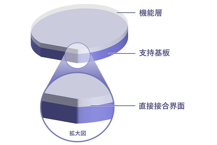
Bonded wafers are substrates for electronic devices fabricated by bonding together differing materials. The two types of substrates are directly bonded without using adhesive and then the functional layer undergoes ultra-precise thin polishing. This enables the addition of physical properties such as high insulation, high thermal conductivity, low thermal expansion, and high rigidity of the base substrate to improve various characteristics including temperature characteristics. Hybrid bonded wafers contribute to creating compact, high-speed, and low power consumption devices for applications such as optical modulators, wavelength conversion devices, and high-power lasers for optical communications. NGK will display TFLN, TFLT, PPLN, and InP/SiC wafers at this exhibition.
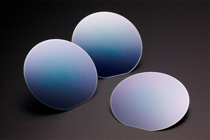
TFLN bonded wafer for optical communications

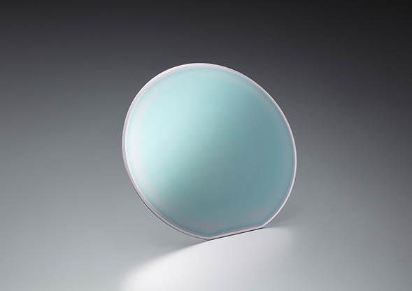
TFLN bonded wafers for optical communications are high-performance wafers made by precision-polishing a bonded wafer consisting of lithium niobate (LN) bonded to a base substrate. This product offers thin-film LN free of crystal damage, which contributes to the development of optical modulation devices featuring lower power consumption and smaller dimensions—ideal for data centers and core/metro networks.
At this exhibition, we will unveil for the first time our newly developed 8‑inch TFLN bonded wafer. While 4‑inch and 6‑inch are commonly available size for the TFLN wafers, achieving 8‑inch large‑diameter is a cutting‑edge progress. This advancement can expand option for foundries of photonics to utilize their existing production lines to scale their production.
InP bonded wafers for high-power lasers
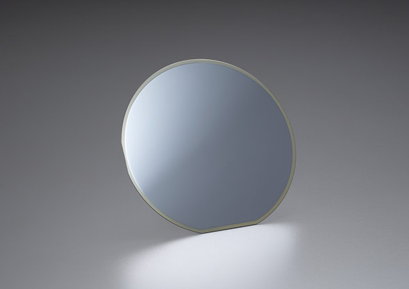
InP bonded wafers for high-power lasers are manufactured by directly bonding InP and SiC, a high heat-dissipating material.
NGK proprietary bonding and polishing technologies can suppress the heat generated by lasers formed on InP wafers. The wafers may be used to build high-power lasers for telecoms and also to build ELS (External Laser Source) used in CPO (Co-Packaged Optices) for AI servers.
High Performance Substrates
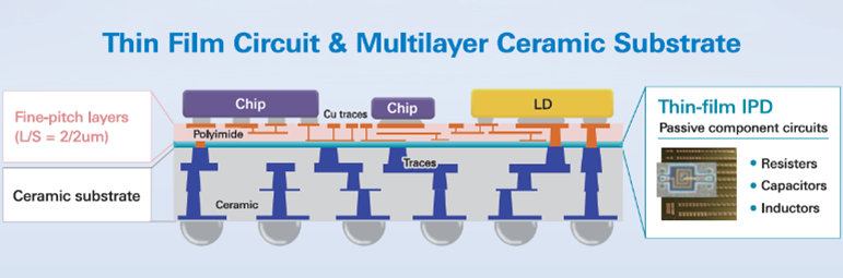
NGK’s substrates support semiconductor devices in various forms used for 5G communication and beyond. The next-generation communication technology requires high-speed, large-capacity, low power, and low latency. In the exhibition, we will showcase substrates designed for next‑generation Optical Engines (OE), Electro‑absorption Modulated Lasers (EML), and External Laser Sources (ELS).